Chapter 4
Bipolar Junction Transistors (BJTs)
In the previous chapter we outlined how the semiconductor diode is described to Spice using a diode element and model statement. Further, we illustrated how the terminal characteristics of a diode are modeled within Spice and how the user can alter the parameters of this model to more closely characterize specific diode behavior. In this chapter on the bipolar junction transistor (BJT) we shall proceed in a similar fashion, first outlining the two statements that are required to describe a BJT to Spice. This will then be followed by a brief description of the model used to represent the BJT within Spice. On completion of this, we shall use Spice to investigate the low-frequency behavior of various types of electronic circuits containing BJTs. The types of circuits that will be simulated will range from single npn and pnp transistor amplifiers to multiple-transistor amplifier circuits, as well as circuits that utilize the transistor as an on-off switch.
4.1 Describing BJTs To Spice
Two statements are required to describe any particular semiconductor device to Spice. One statement is necessary to describe the nature of the semiconductor device and the manner in which it is connected to the rest of the network, and the other statement is required to describe the parameters of the built-in model of the semiconductor device described by the first statement. In the following we shall describe these two statements as they apply to the BJT.
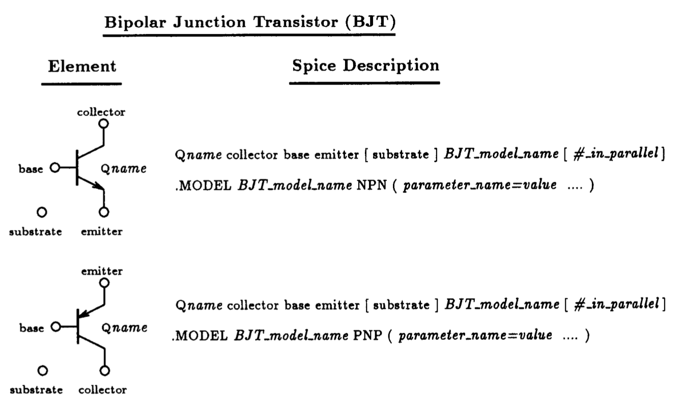
Fig. 4.1: Spice element description for the npn and pnp BJT. Also listed is the general form of the associated BJT model statement. A partial listing of the parameter values applicable to either the npn or pnp BJT given in Table 4.1.
4.1.1 BJT Element Description
The presence of a BJT in a circuit is described to Spice through the Spice input file using an element statement beginning with the letter Q. If more than one transistor exists in a circuit, then a unique name must be attached to Q to uniquely identify each transistor. This is then followed by a list of the three nodes to which the collector, base, and emitter of the BJT are connected to. One can also include the node that the substrate is connected to if it is an integrated transistor. Subsequently, on the same line, the name of the model that will be used to characterize this particular BJT is given. The name of this model must correspond to the name given on a model statement containing the parameter values that characterize this transistor to Spice. Lastly, one has the option of specifying the number of BJTs that are considered to be connected in parallel.
For quick reference we depict the syntax for the Spice statement describing the BJT in Fig. 4.1. Also shown is the syntax for the model statement (.MODEL) that must be present in any Spice input file that makes reference to the built-in BJT model of Spice. This statement defines the terminal characteristics of the BJT by specifying the values of particular parameters of the BJT model. We shall discuss the model statement more fully next.
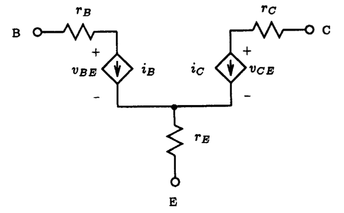
Fig. 4.2: The Spice large-signal BJT model for DC analysis.
4.1.2 BJT Model Description
As is evident from Fig. 4.1, the model statement for either the npn or pnp transistor begins with the keyword .MODEL and is followed by the name of the model used by a BJT element statement, the nature of the BJT (i.e., npn or pnp), and a list of the parameters characterizing the terminal behavior of the BJT, enclosed between brackets. The number of parameters associated with the Spice model of the BJT is rather large (40 in total), and their individual meanings are rather involved. Instead of trying to describe the meaning of each parameter of the BJT model, we shall simply outline the parameters of the Spice BJT model that are relevant to the discussion contained within this chapter.
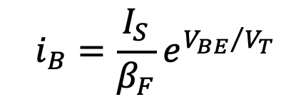
The Spice BJT model is illustrated schematically in Fig. 4.2. The ohmic resistances of the base, collector, and emitter regions of the BJT are lumped into three linear resistances rB, rC and rE, respectively. The DC characteristics of the intrinsic BJT are determined by the nonlinear dependent current sources iB and iC. The exact functional descriptions of these two currents - as adopted by Spice - are rather complex and will not be given here. Interested readers can consult [Nagel, 1975] for more details. For a transistor operated in its active mode, a first-order representation of these two currents can be described by the following two equations
(4.1)
and
(4.2)
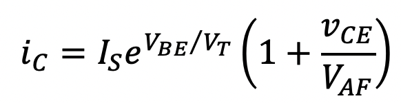
Here IS is the saturation current (similar to the diode saturation current) and VT is the thermal voltage. The constant BF is the forward common-emitter current gain. In Sedra and Smith, this constant is designated simply as B. Spice attaches the subscript F to distinguish BF from another current gain BR which represents the common-emitter current gain of the same transistor when operated in the reverse mode (that is, with the emitter and collector interchanged). Finally, VAF is the forward early voltage (denoted VA in Sedra and Smith).
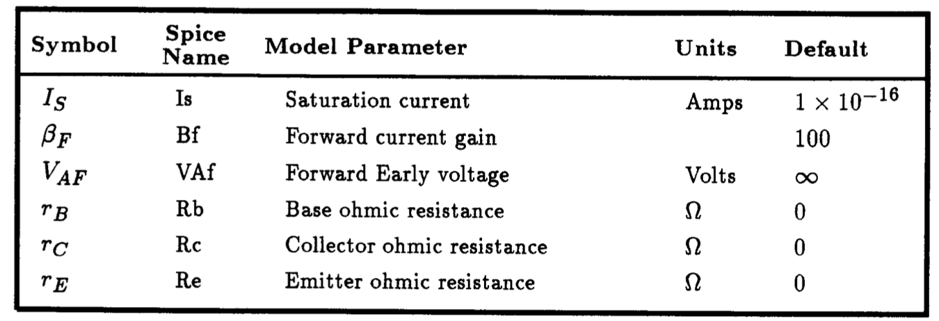
Table 4.1: A partial listing of the Spice parameters for a static BJT model.
A partial listing of the parameters associated with the Spice BJT model under static conditions is given in Table 4.1. Also listed are the associated default values; if the value of a particular parameter is not specified on the .MODEL statement, the parameter assumes its default value. To specify a parameter value one simply writes, for example, Is=1e-14, Bf=100, etc..
4.1.3 Verifying NPN Transistor Circuit Operation
As the first example of this chapter, consider verifying the npn transistor circuit designed in Example 4.1 of Sedra and Smith and repeated here in Fig. 4.3. This particular transistor circuit was designed to have a collector current of 2 mA and a collector voltage of +5 V.
For the purpose of design, the npn transistor was assumed to have a BF = 100 and to exhibit a vBE of 0.7 V at iC = 1 mA. The first condition can be directly specified on the BJT model statement using BF=100, however, the latter condition needs to be translated into a BJT parameter. From Eqn. (4.2) we can write
(4.3)
![]()
Now, to make matters simpler, we shall assume that VAF = infinity, thus reducing the above equation to
(4.4)
![]()
We can then solve to obtain IS=1.8104 x 10⁻¹⁵ A. Our model statement for this particular transistor is then described to Spice using the following statement:
.model npn_transistor npn (Is=1.8104e-15 Bf=100) .
Notice that we did not specify the value of VAF in the list of parameters, rather, we are relying on the default value assigned to VAF. Of course, the same could have also been done for the parameter BF.
|
Fig. 4.3: Transistor circuit design created by Sedra and Smith in Example 4.1 of their text. Spice is used to calculate the DC operating point of this circuit.
|
Example 4.1: Verifying Transistor Circuit Design
** Circuit Description ** Vcc 1 0 DC +15V Vee 4 0 DC -15V Q1 2 0 3 npn_transistor Rc 1 2 5k Re 3 4 7.07k * transistor model statement .model npn_transistor npn (Is=1.8104e-15 Bf=100) ** Analysis Requests ** * calculate DC bias point information .OP ** Output Requests ** * none required .end
Fig. 4.4: The Spice input file for calculating the collector current and voltage of the transistor circuit shown in Fig. 4.3.
|

Assuming the nodes of the circuit are labeled as shown in Fig. 4.3, the corresponding Spice input file is listed in Fig. 4.4. An operating point analysis command (.OP) is included in this file to tell Spice to calculate the DC operating point of this circuit. Submitting this file to Spice, results in the following DC operating point information:
|
**** SMALL SIGNAL BIAS SOLUTION TEMPERATURE = 27.000 DEG C ****************************************************************************
NODE VOLTAGE NODE VOLTAGE NODE VOLTAGE NODE VOLTAGE
( 1) 15.0000 ( 2) 4.9990 ( 3) -.7172 ( 4) -15.0000
VOLTAGE SOURCE CURRENTS NAME CURRENT
Vcc -2.000E-03 Vee 2.020E-03
TOTAL POWER DISSIPATION 6.03E-02 WATTS
|
As is evident, the collector of the transistor (node 2) is at 4.9990 V and the collector current IC, as inferred from the current supplied by the voltage source VCC is 2.000 mA. (The negative sign is a result of the convention used by Spice). Although, the collector voltage is not exactly at +5 V, the deviation from this value is extremely small (1 mV). If one were to back-track to find why this error occurred, one would find that the value of VT=25 mV assumed during the design phase is different than the value of VT=25.89 mV that Spice used, assuming a circuit temperature of 27°C. Repeating the design procedure outlined in Example 4.1 with the exact value of VT=25.89 mV would result in an emitter resistance of RE=7.0703 k-ohm and a collector voltage much closer to +5 V.
4.2 Using Spice as a Curve Tracer
A typical curve-tracer arrangement for measuring the iC - vCE characteristics of a transistor is illustrated in Fig. 4.5. Here two independent sources vCE and iB are varied, and the collector current of the transistor is calculated. The collector current would then be plotted as a function of vCE and iB. For example, consider plotting the forward iC - vCE characteristics of a npn transistor characterized by IS=1.8104 x 10⁻¹⁵ A, BF=100, and a forward Early voltage VAF=35 V, for a base current of 10 uA. Using the circuit displayed in Fig. 4.5 as a guide, we can create the Spice input file shown in Fig. 4.6 to accomplish this task. We make use of the DC Sweep command available in Spice to vary the collector-emitter voltage of transistor Q1 from 0 V to +10 V in 100 mV steps. The resulting iC - vCE characteristic as calculated by Spice is displayed in Fig. 4.7.
|
Fig. 4.5: Spice curve-tracer arrangement for calculating the iC - vCE characteristics of a BJT.
|
Spice As A Curve Tracer: BJT I-V Characteristics
** Circuit Description ** Vce 1 0 DC 0V Ib 0 2 DC 10uA * device under test Q1 1 2 0 npn_transistor * transistor model statement .model npn_transistor NPN (Is=1.8104e-15A Bf=100 VAf=35V) ** Analysis Requests ** * vary Vce from 0V to 10V in steps of 100mV .DC Vce 0V +10V 100mV ** Output Requests ** .plot DC I(Vce) .probe .end
Fig. 4.6: The Spice input file for calculating the collector current of the transistor circuit shown in Fig. 4.5 for a given base current and collector-emitter voltage.
|

Typically, one also wants to vary the base current iB while at the same time varying vCE of the transistor. This can be accomplished with Spice by augmenting the DC Sweep command with another source name and the range of values it should be stepped through. For example, the DC Sweep command required to sweep vCE from 0 V to +10 V in 100 mV steps while at the same time sweeping iB from 1 uA to 10 uA in 1 uA steps is simply the following:
.DC Vce 0V +10V 100mV Ib 1u 10u 1u.
In essence, this command tells Spice to perform the voltage sweep for each value specified by the current sweep. (For those familiar with computer programming, this command should remind them of a set of programming loops: the inner sweep being nested within the outer sweep.)
Revising the Spice input deck with this augmented DC Sweep command and re-submitting this job to Spice, the iC - vCE characteristics displayed in Fig. 4.8 are obtained. Clearly, other arrangements of the two independent sources are possible, thus allowing one to investigate other characteristics of the transistor. We encourage the reader to investigate some of them using the approach just outlined.
|
Fig. 4.7: The iC - vCE curve at a base current of 10 uA for a transistor characterized by IS=1.8104 x 10⁻¹⁵ A, BF=100, and VAF=35 V.
|
Fig. 4.8: A family of iC - vCE curves for a base current varied between 1 uA and 10 uA in steps of 1 uA for a transistor characterized by IS=1.8104 x 10⁻¹⁵ A, BF=100, and VAF=35 V.
|


4.3 Spice Analysis of Transistor Circuits At DC
We are now ready to investigate the DC operating point of several simple transistor circuits using Spice. Throughout this section we shall assume that the transistor is characterized by a BF=100, exhibits a vBE of 0.7 V at iC=1 mA, and that its Early voltage is infinite. The primary goal of this section is to determine, with the aid of Spice, the mode of operation that a transistor is working in.
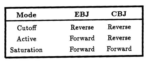
Table 4.2: BJT modes of operation.
4.3.1 Transistor Modes of Operation
Depending on the bias condition imposed across the emitter-base junction (EBJ) and the collector-base junction (CBJ), different modes of operation of the BJT are obtained, as shown in Table 4.2. In the following we shall look at several transistor circuits and use Spice to determine the mode of operation of each.
Active Region
Consider the circuit shown in Fig. 4.9. This same circuit was analyzed by Sedra and Smith using hand analysis in Example 4.2 of their text and transistor Q1 was shown to be operating in the active region. We shall repeat this example using Spice to calculate the DC operating point and show that, indeed, transistor Q1 is operating in the active mode.
|
Fig. 4.9: A simple npn transistor circuit (Example 4.2 of Sedra and Smith).
|
Example 4.2: NPN Transistor Operated In Active Mode
** Circuit Description ** Vcc 1 0 DC +10V Vbb 3 0 DC +4V Q1 2 3 4 npn_transistor Rc 1 2 4.7k Re 4 0 3.3k * transistor model statement .model npn_transistor npn (Is=1.8104e-15 Bf=100) ** Analysis Requests ** * calculate DC bias point information .OP ** Output Requests ** * none required .end
Fig. 4.10: The Spice input file for calculating the DC operating point of the circuit shown in Fig. 4.9.
|

A Spice description of this circuit is listed in Fig. 4.10 and a DC operating point analysis request is included. The results of the analysis are listed below:
|
**** SMALL SIGNAL BIAS SOLUTION TEMPERATURE = 27.000 DEG C ****************************************************************************
NODE VOLTAGE NODE VOLTAGE NODE VOLTAGE NODE VOLTAGE
( 1) 10.0000 ( 2) 5.3452 ( 3) 4.0000 ( 4) 3.3009
**** OPERATING POINT INFORMATION TEMPERATURE = 27.000 DEG C ****************************************************************************
**** BIPOLAR JUNCTION TRANSISTORS
NAME Q1 MODEL npn_transistor IB 9.90E-06 IC 9.90E-04 VBE 6.99E-01 VBC -1.35E+00 VCE 2.04E+00
|
Included amongst the list of node voltages is a partial summary of the DC operating point conditions associated with the transistor. This includes the currents IB and IC, and the voltages VBE, VBC, and VCE. Other information is included in this list of operating point information but is not shown here. Also, we do not show the small-signal parameters associated with the hybrid-pi model of the transistor, deferring discussion of this topic to a later stage.
What one should notice here, amongst this operating point information, is that the base-emitter junction is forward biased with VBE=0.699 V and the collector-base junction is reversed biased with VBC=-1.35 V; thus confirming that transistor Q1 is indeed operating in its active region. One could have deduced this same information from the DC node voltages, but for multiple transistor circuits this can be a tedious endeavor. Also, the collector and base currents agree reasonably well with the values calculated by hand analysis.
Saturation Region
If we increase the base voltage of the circuit of Fig. 4.11 from +4 V to +6 V, transistor Q1 leaves the active region and moves into the saturation region. To see this, change the value of Vbb in the Spice input file shown in Fig. 4.10 to +6 V and re-run the Spice job. The results are:
|
**** SMALL SIGNAL BIAS SOLUTION TEMPERATURE = 27.000 DEG C ****************************************************************************
NODE VOLTAGE NODE VOLTAGE NODE VOLTAGE NODE VOLTAGE
( 1) 10.0000 ( 2) 5.3147 ( 3) 6.0000 ( 4) 5.2808
**** OPERATING POINT INFORMATION TEMPERATURE = 27.000 DEG C ****************************************************************************
**** BIPOLAR JUNCTION TRANSISTORS
NAME Q1 MODEL npn_transistor IB 6.03E-04 IC 9.97E-04 VBE 7.19E-01 VBC 6.85E-01 VCE 3.39E-02
|
As is evident, both VBE and VBC are forward biased, suggesting that Q1 is operating in its saturation region. The saturation region of operation will be studied further in Sections 4.4 and 4.5.
Cutoff Region
Finally, if we reduce the base voltage to zero volts, then the transistor becomes cutoff. Altering the Spice input deck to reflect this (i.e., setting Vbb=0) and re-running the Spice job results in the
following:
|
**** SMALL SIGNAL BIAS SOLUTION TEMPERATURE = 27.000 DEG C ****************************************************************************
NODE VOLTAGE NODE VOLTAGE NODE VOLTAGE NODE VOLTAGE
( 1) 10.0000 ( 2) 10.0000 ( 3) 0.0000 ( 4) 33.01E-09
**** OPERATING POINT INFORMATION TEMPERATURE = 27.000 DEG C ****************************************************************************
**** BIPOLAR JUNCTION TRANSISTORS
NAME Q1 MODEL npn_transistor IB -1.00E-11 IC 2.00E-11 VBE -3.30E-08 VBC -1.00E+01 VCE 1.00E+01
|
Here, both VBE and VBC are reversed biased, indicating that Q1 is now cutoff. Notice, however, that even under cutoff conditions the transistor is still conducting a base and collector current (and, of course, an emitter current). These currents are mainly leakage currents associated with the two reverse biased junctions of the transistor.
|
Fig. 4.11: A simple pnp transistor circuit (Example 4.5 of Sedra and Smith).
|
Example 4.5: PNP Transistor DC Operating Point Calculation
** Circuit Description ** Vcc 1 0 DC +10V Vee 4 0 DC -10V Q1 3 0 2 pnp_transistor Re 1 2 2k Rc 3 4 1k * transistor model statement .model pnp_transistor pnp (Is=1.8104e-15 Bf=100) ** Analysis Requests ** * calculate DC bias point information .OP ** Output Requests ** * none required .end
Fig. 4.12: The Spice input file for calculating the DC operating point of the circuit shown in Fig. 4.11.
|

4.3.3 Computing DC Bias of a PNP Transistor Circuit
The above circuit examples consisted of npn transistors only. In this next example we shall calculate the DC operating point of a circuit containing a pnp transistor. As far as Spice is concerned, pnp transistor circuits are no more complicated than npn transistor circuits.
Consider the circuit shown in Fig. 4.11. This example corresponds to Example 4.5 of Sedra and Smith, 3rd Edition. The Spice input file for this circuit is listed in Fig. 4.12 and the results of the DC analysis are shown below:
|
**** SMALL SIGNAL BIAS SOLUTION TEMPERATURE = 27.000 DEG C ****************************************************************************
NODE VOLTAGE NODE VOLTAGE NODE VOLTAGE NODE VOLTAGE
( 1) 10.0000 ( 2) .7387 ( 3) -5.4152 ( 4) -10.0000
VOLTAGE SOURCE CURRENTS NAME CURRENT
Vcc -4.631E-03 Vee 4.585E-03
TOTAL POWER DISSIPATION 9.22E-02 WATTS
**** OPERATING POINT INFORMATION TEMPERATURE = 27.000 DEG C ****************************************************************************
**** BIPOLAR JUNCTION TRANSISTORS
NAME Q1 MODEL pnp_transistor IB -4.58E-05 IC -4.58E-03 VBE -7.39E-01 VBC 5.42E+00 VCE -6.15E+00
|
From the above results, it is obvious that the transistor is operating in the active mode. Notice that the polarity of the transistor currents is opposite to those of a npn transistor operating in its active region (see the previous subsection). Further, one should also note that Spice defines a positive collector current of a pnp transistor as the current flowing into the collector. This is opposite to that which Sedra and Smith uses. One should be careful of this. When one compares the above Spice results with those generated by a simple hand calculation, say, for example, as was performed in Example 4.5 of Sedra and Smith, we find we are in very good agreement; about a 0.4% difference.
In the above analysis, the Early effect was neglected. In practise this is never the case. In the following, let us repeat the above analysis assuming the pnp transistor has an Early voltage VAF of 100 V. We shall then compare the resulting transistor collector current with that obtained previously when the Early effect was ignored.
Consider replacing the transistor model statement for the pnp transistor given in the Spice deck of Fig. 4.12 with the following one:
.model pnp_transistor pnp (Is=1.8104e-15 Bf=100 Vaf=100V).
Re-running the Spice job, we find in the Spice output file the following results:
|
**** SMALL SIGNAL BIAS SOLUTION TEMPERATURE = 27.000 DEG C ******************************************************************************
NODE VOLTAGE NODE VOLTAGE NODE VOLTAGE NODE VOLTAGE
( 1) 10.0000 ( 2) .7373 ( 3) -5.4122 ( 4) -10.0000
VOLTAGE SOURCE CURRENTS NAME CURRENT
Vcc -4.631E-03 Vee 4.588E-03
**** OPERATING POINT INFORMATION TEMPERATURE = 27.000 DEG C ******************************************************************************
**** BIPOLAR JUNCTION TRANSISTORS
NAME Q1 MODEL pnp_transistor IB -4.35E-05 IC -4.59E-03 VBE -7.37E-01 VBC 5.41E+00 VCE -6.15E+00
|
We see from the above results that the collector current is now 4.59 mA. This is in contrast to the previous situation when the Early effect was ignored, and a Spice analysis revealed a collector current of 4.58 mA. In the latter case, a similar result would also be obtained by a simple hand calculation, as was noted above. Thus, if we compare the result obtained by Spice with the Early effect included to that obtained by a simple hand calculation, we see a difference of about 0.2%. For most practical engineering situations, a 5% to 10% accuracy obtained from a simple hand analysis is usually quite acceptable. But, more importantly, to account for the Early effect during hand analysis would complicate the analysis significantly that it would probably mask any insight. Thus, if greater accuracy is thought necessary then one should make use of a detailed Spice analysis with the transistor Early effect included.
|
Fig. 4.13: A multiple transistor circuit (Example 4.8 of Sedra and Smith).
|
Example 4.8: Multiple Transistor Circuit Bias Point Calculation
** Circuit Description ** Vcc 1 0 DC +15V * npn stage Q1 2 3 4 npn_transistor Rc 1 2 5k Rb1 1 3 100k Rb2 3 0 50k Re 4 0 3k * pnp stage Q2 6 2 5 pnp_transistor Re2 1 5 2k Rc2 6 0 2.7k * transistor model statement .model npn_transistor npn (Is=1.8104e-15 Bf=100) .model pnp_transistor pnp (Is=1.8104e-15 Bf=100) ** Analysis Requests ** * calculate DC bias point information .OP ** Output Requests ** * none required .end
Fig. 4.14: The Spice input file for calculating the DC operating point of the multiple transistor circuit shown in Fig. 4.13.
|

4.3.4 DC Operating Point of a Multiple Transistor Circuit
Consider the multiple transistor circuit shown in Fig. 4.13. This same circuit was analyzed by hand for its node voltages and branch currents by Sedra and Smith, 3rd Edition, and designated as Example 4.8 in their text. We shall compute the DC operating point of this circuit using Spice. The Spice input file is listed in Fig. 4.14 with an operating point analysis command included. The results generated by Spice are listed below:
|
**** SMALL SIGNAL BIAS SOLUTION TEMPERATURE = 27.000 DEG C ****************************************************************************
NODE VOLTAGE NODE VOLTAGE NODE VOLTAGE NODE VOLTAGE
( 1) 15.0000 ( 2) 8.7526 ( 3) 4.5744 ( 4) 3.8688 ( 5) 9.4779 ( 6) 7.3810
VOLTAGE SOURCE CURRENTS NAME CURRENT
Vcc -4.115E-03
TOTAL POWER DISSIPATION 6.17E-02 WATTS
**** OPERATING POINT INFORMATION TEMPERATURE = 27.000 DEG C ****************************************************************************
**** BIPOLAR JUNCTION TRANSISTORS
NAME Q1 Q2 MODEL npn_transistor pnp_transistor IB 1.28E-05 -2.73E-05 IC 1.28E-03 -2.73E-03 VBE 7.06E-01 -7.25E-01 VBC -4.18E+00 1.37E+00 VCE 4.88E+00 -2.10E+00
|
Comparing these results with those calculated by hand in Sedra and Smith, we see that the results generated by hand analysis (e.g., IC1= 1.28 mA and IC2= 2.75 mA) are quite close to the values generated by Spice. Moreover, we see that both transistors are operating in the active mode.
In the following we repeat the analysis with each transistor having an Early voltage of 100 V. This requires that we modify the two-transistor model statement given in the Spice deck of Fig. 4.14 to the following:
.model npn_transistor npn (Is=1.8104e-15 Bf=100 Vaf=100V)
.model pnp_transistor pnp (Is=1.8104e-15 Bf=100 Vaf=100V)
On doing so, and re-submitting the revised Spice deck for processing, we obtain the following results:
|
**** SMALL SIGNAL BIAS SOLUTION TEMPERATURE = 27.000 DEG C ******************************************************************************
NODE VOLTAGE NODE VOLTAGE NODE VOLTAGE NODE VOLTAGE
( 1) 15.0000 ( 2) 8.7227 ( 3) 4.5894 ( 4) 3.8847 ( 5) 9.4478 ( 6) 7.4222
VOLTAGE SOURCE CURRENTS NAME CURRENT
Vcc -4.136E-03
TOTAL POWER DISSIPATION 6.20E-02 WATTS
**** OPERATING POINT INFORMATION TEMPERATURE = 27.000 DEG C ******************************************************************************
**** BIPOLAR JUNCTION TRANSISTORS
NAME Q1 Q2 MODEL npn_transistor pnp_transistor IB 1.23E-05 -2.71E-05 IC 1.28E-03 -2.75E-03 VBE 7.05E-01 -7.25E-01 VBC -4.13E+00 1.30E+00 VCE 4.84E+00 -2.03E+00
|
Here we see that the collector current of Q1 remains at 1.28 mA, but the collector current of Q2 has increased to a level of 2.75 mA, a 0.02 mA increase. This example, like the previous one, demonstrates the effect that transistor Early voltage has on the DC bias levels in a circuit and shows that it is usually small. Thus, not accounting for it during a hand analysis seems reasonable.
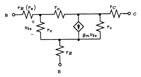
Fig. 4.15: The small-signal BJT Spice model under static conditions.
4.4 BJT Transistor Amplifiers
Transistors operated in their active region find important applications as linear amplifiers. Design and analysis of linear amplifiers is facilitated by the use of small-signal models for the BJT. In the following we discuss the small-signal model used by Spice.
4.4.1 BJT Small-Signal Model
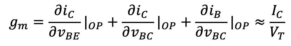
Under static and small-signal conditions, the linearized BJT Spice model is the familiar hybrid-pi model shown in Fig. 4.15. Both the npn and pnp transistor have the same hybrid-pi model, so we make no distinction between the two. The transconductance gm is related to the DC bias current IC according to the following
(4.5)
Similarly, the input and output resistances are also related to the transistors DC operating point, according to the following
(4.6)

(4.7)
and ru is approximated as
(4.8)
Also included in the hybrid-model are the ohmic resistances of the three junctions; rC, rB (rx), and rE. Note that rE is not the re used in the text by Sedra and Smith.
The small-signal parameters of a transistor are usually computed by Spice prior to most analyses. In many types of analysis, the small-signal model of the BJT is paramount to the analysis. Spice will list the small-signal model parameters of all transistors in a given circuit when an .OP command is included in the Spice input file. Because of the importance of the base resistance rB on small-signal operation, Spice will also list this value amongst the small-signal parameters in the output file. It will be denoted by Rx.
As an example of the small-signal parameters that are listed in the Spice output file as a result of an .OP analysis command, we show below the operating point information for transistors Q1 and Q2 in our previous example given in subsection 4.3.3:
|
**** BIPOLAR JUNCTION TRANSISTORS
NAME Q1 Q2 MODEL npn_transistor pnp_transistor IB 1.23E-05 -2.71E-05 IC 1.28E-03 -2.75E-03 VBE 7.05E-01 -7.25E-01 VBC -4.13E+00 1.30E+00 VCE 4.84E+00 -2.03E+00 BETADC 1.04E+02 1.01E+02 GM 4.96E-02 1.06E-01 RPI 2.10E+03 9.53E+02 RX 0.00E+00 0.00E+00 RO 8.12E+04 3.69E+04 CBE 0.00E+00 0.00E+00 CBC 0.00E+00 0.00E+00 CBX 0.00E+00 0.00E+00 CJS 0.00E+00 0.00E+00 BETAAC 1.04E+02 1.01E+02 FT 7.89E+17 1.69E+18
|
Here we see a list containing the DC operating point and small-signal model parameters for both the npn and pnp transistors in the circuit of Fig. 4.13. Besides the parameters that have already been explained, this list also contains other parameters, such as capacitances CBE, CBC, CBX and CJS. These capacitances model dynamic effects of the transistor and will be further explained in Chapter 7. Likewise, BETAAC, and FT, are parameters that are derived from the dynamic small-signal model of the transistor and will also be explained in Chapter 7.
4.4.2 Single-Stage Voltage-Amplifier Circuits
Consider the voltage amplifier circuit shown in Fig. 4.16. This circuit was presented and analyzed for its voltage gain by Sedra and Smith in Example 4.9 of their text. Here we shall use Spice to calculate the voltage gain of this circuit assuming that the transistor has a BF = 100 and IS=1.8104 x 10⁻¹⁵ A. The other parameters of the BJT model will take on their default values.
|
Fig. 4.16: A simple common-emitter voltage amplifier (Example 4.9 of Sedra and Smith).
|
Example 4.9: Calculating Voltage Gain Of A Transistor Amplifier
** Circuit Description ** * dc supplies Vcc 1 0 DC +10V Vbb 5 0 DC +3V * small-signal input Vi 4 5 DC 1mV * amplifier circuit Q1 2 3 0 npn_transistor Rc 1 2 3k Rbb 4 3 100k * transistor model statement .model npn_transistor npn (Is=1.8104e-15 Bf=100) ** Analysis Requests ** * calculate small-signal transfer function: Vo/Vi .TF V(2) Vi * we shall also calculate the small-signal parameters of the transistor .OP ** Output Requests ** * none required .end
Fig. 4.17: The Spice input file for calculating the small-signal voltage gain of the circuit shown in Fig. 4.16.
|

In Fig. 4.17 we list the Spice input file for this circuit. A transfer function command (.TF) is included to calculate the voltage gain vo/vi where vo is taken at node 2. In addition, we are also requesting an operating point calculation (.OP) so that we may cross-check the results found using the .TF command with those computed by hand using the equations derived by Sedra and Smith, 3rd Edition, in Example 4.9 of their text.
The results of the .TF command are as follows:
|
**** SMALL-SIGNAL CHARACTERISTICS
V(2)/Vi = -2.966E+00
INPUT RESISTANCE AT Vi = 1.011E+05
OUTPUT RESISTANCE AT V(2) = 3.000E+03
|
Hence, the voltage gain of this circuit is -2.966 V/V. Also, the input and output resistance of this circuit are 101.1 k-ohm and 3 k-ohm, respectively. Referring back to the circuit shown in Fig. 4.16, these resistance levels seem to be in line with what one would expect.
We can collaborate the voltage gain calculation found using the .TF command by performing the same gain calculation using the small-signal equivalent circuit representation of the amplifier circuit shown in Fig. 4.16. This was performed by Sedra and Smith, and they found that the voltage gain, in terms of the small-signal parameters of the transistor, is given by
(4.9)
![]()
In this derivation the output resistance of the transistor was assumed infinite. The small-signal parameters of the hybrid-pi model for this particular transistor as calculated by Spice are found amongst the transistor operating point information in the Spice output file. A partial listing of the operating point information found in the output file for transistor Q1 is given below:
|
**** BIPOLAR JUNCTION TRANSISTORS
NAME Q1 MODEL npn_transistor IB 2.28E-05 IC 2.28E-03 VBE 7.21E-01 VBC -2.44E+00 VCE 3.16E+00 BETADC 1.00E+02 GM 8.82E-02 RPI 1.13E+03 RX 0.00E+00 RO 1.00E+12
|
From the above list, we see that gm=88.2 mA/V and rp=1.13 k-ohm. Substituting these values, together with RC=3 k-ohm and RBB=100 k-ohm, into Eqn. (4.9), one finds the voltage gain to be -2.96 V/V. Comparing this result with that computed using the .TF command of Spice, as expected, one finds almost exact agreement. The difference is due the number of significant digits used in the two calculations. In principle, these two calculations should be in perfect agreement because the .TF command calculates the voltage gain in the exact same way.
|
Fig. 4.16: A simple common-emitter voltage amplifier (duplicate).
|
Example 4.10: Time-Domain Waveforms Of A Transistor Amplifier
** Circuit Description ** * dc supplies Vcc 1 0 DC +10V Vbb 5 0 DC +3V * small-signal input Vi 4 5 PULSE (-1.1V 1.1V 0 0.5ms 0.5ms 1us 1ms) * amplifier circuit Q1 2 3 0 npn_transistor Rc 1 2 3k Rbb 4 3 100k * transistor model statement .model npn_transistor npn (Is=1.8104e-15 Bf=100) ** Analysis Requests ** .TRAN 10us 4ms 0ms 10us ** Output Requests ** .PLOT TRAN V(2) .probe .end
Fig. 4.18: The Spice input file for calculating the collector voltage of the circuit shown in Fig. 4.16 subject to a triangular waveform input.
|

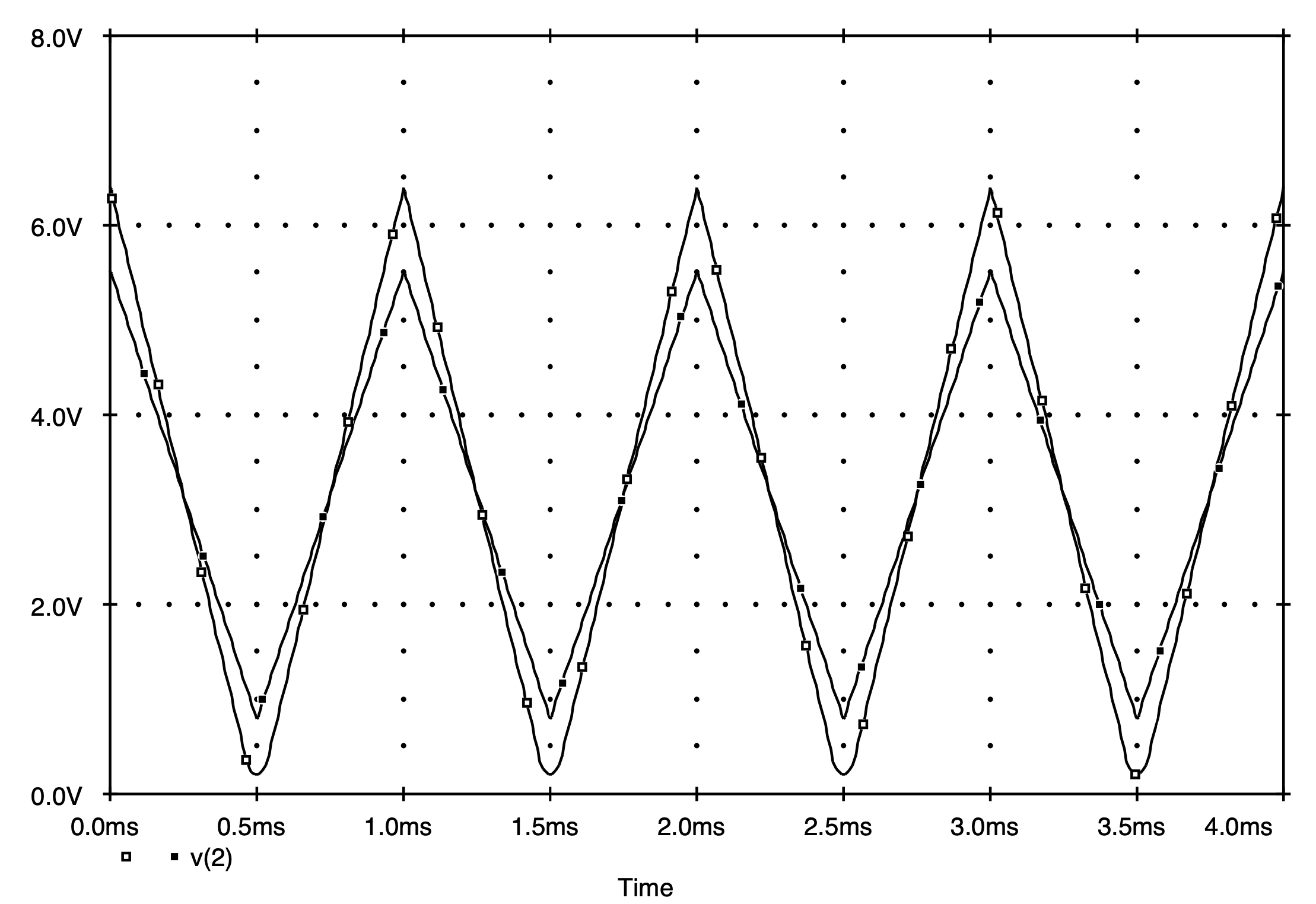
Fig. 4.19: The output voltage waveform of the amplifier shown in Fig. 4.16 for two different inputs levels of 0.8 V and 1.1 V. The larger output signal is seen to be clipped on its lower peaks.
To visualize the operation of this amplifier, consider simulating the circuit shown in Fig. 4.16 with a time-varying input. More specifically, we shall consider that vi is time-varying with a triangular waveform. We shall consider that the input signal has a period of 1 ms and an input amplitude of 1.1 V. Moreover, we shall repeat the same example with the input amplitude reduced to 0.8 V. We shall then want to compare the results.
To emulate a triangular waveform, we make use of the following PULSE statement:
Vi 4 5 PULSE (-1.1V 1.1V 0 0.5ms 0.5ms 1us 1ms)
The rise and fall times are set to equal half the period of the triangle waveform of 1 ms. Mathematically, the pulse width field should be zero, however, due to a Spice technicality, the pulse width cannot be specified as being equal to zero. To circumvent this problem, we set the pulse width to a small, but, nonzero value - in this case 1 us. Furthermore, we added a .TRAN statement to calculate the time response of the circuit over a 4 ms interval. The resulting Spice input file for the first example is listed in Fig. 4.18. The same file can be used for the second case by simply reducing the peak level of the input signal from 1.1 V to 0.8 V. For comparison purposes, we shall concatenate the two files together before submitting the job to Spice.
The voltage waveforms at the collector of the amplifier for both input levels, as calculated by Spice, are displayed in Fig. 4.19. Both signals are riding on a DC component of 3.2 V, corresponding to the DC bias point at the collector. One will also notice that the larger output waveform is clipped on its lower peak. This can be traced back to the transistor being forced into its cutoff region when the input signal level exceeds a 0.82 V level. The other waveform does not appear to be clipped, confirming that the transistor stays out of its cutoff region.
Another Example:
As another example of a transistor being used to form a linear amplifier, consider the circuit shown in Fig. 4.20. In this particular case, a pnp transistor is the central component of the design. This circuit was analyzed by hand by Sedra and Smith, 3rd Edition, in Example 4.11 of their text. From their analysis they found that the amplifier had a noninverting voltage gain of 183.3 V/V. They reasoned that, because the input signal appears directly across the base-emitter junction of the pnp transistor, the input signal amplitude must remain below 10 mV to justify small-signal operation and obtain this voltage gain. In the following we shall simulate the amplifier circuit shown in Fig. 4.20 subject to a triangular waveform input signal having a peak value of 10 mV and compare it to one with twice the amplitude.
The Spice input file for the pnp transistor amplifier circuit shown in Fig. 4.20 subject to a 10-mV triangular input signal is listed below in Fig. 4.21. The infinite-valued capacitors, C1 and C2, are represented in the Spice input file by large 100 uF capacitors that are initially charged to the DC bias voltage that will eventually appear across them. These are usually found by first determining the DC operating point of the circuit using an .OP command with the input set to zero. This ``trick'' speeds up the circuit simulation by starting the circuit off near its steady-state operation. If these initial conditions were not specified, then our transient simulation time would be excessively long. This stems from the fact that these large coupling capacitors form large time-constants and need a long time to charge to their steady-state values. Even then, we are still required to allot some simulation time for the circuit to reach its true steady-state operation. This is the reason for delaying the output on the .TRAN statement until 10 ms (or 10 periods of the input signal) after its start. Also note that we must specify on the .TRAN statement that we want Spice to use the initial conditions established for each capacitor by specifying the field flag UIC.
Submitting this file, concatenated together with another file having a triangular input signal of 20 mV amplitude, to Spice results in the input and output waveforms shown in Fig. 4.22. The larger output signal in the lower trace due to the 20-mV input signal clearly deviates from an ideal triangle waveform; it looks more parabolic than linear. The smaller output signal caused by the 10-mV input signal though much more linear, exhibits some deviation from the ideal, thus suggesting that the small-signal linear range of operation is actually less than 10 mV.
We also see from Fig. 4.22 that for the 10-mV peak input signal, the corresponding output signal has a peak to peak excursion of 3.5 V, corresponding to a signal gain of 175 V/V. This result is, therefore, in good agreement with the small-signal gain that was calculated by hand (183.3 V/V) in Example 4.11 of Sedra and Smith, 3rd Edition.
|
Fig. 4.20: A pnp transistor amplifier circuit (Example 4.11 of Sedra and Smith).
|
Example 4.11: Time-Domain Waveforms For A PNP Transistor Amplifier
** Circuit Description ** * dc supplies V+ 1 0 DC +10V V- 5 0 DC -10V * small-signal triangular-wave input Vi 3 0 PULSE (-10mV 10mV 0 0.5ms 0.5ms 1us 1ms) * amplifier circuit Q1 4 0 2 pnp_transistor Rc 4 5 5k Re 1 2 10k * dc blockers - very large capacitors C1 3 2 100uF IC=-0.6972V C2 4 6 100uF IC=-5.3946V * output node (very large resistance as not to load the amplifier) Ro 6 0 100Meg * transistor model statement .model pnp_transistor pnp (Is=1.8104e-15 Bf=100) ** Analysis Requests ** * calculate transient response using initial conditions .TRAN 100us 14ms 10ms 100us UIC ** Output Requests ** .PLOT TRAN V(4) V(3) .probe .end
Fig. 4.21: The Spice input file for calculating the input and output signal waveforms of the circuit shown in Fig. 4.20.
|

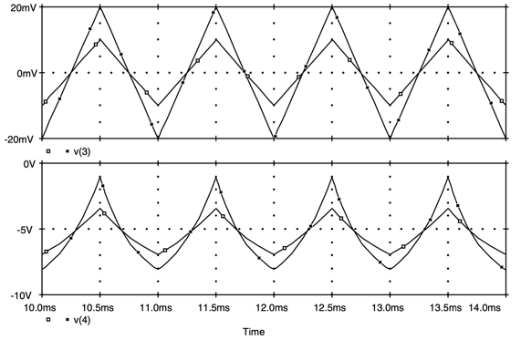
Fig. 4.22: Input and output waveforms of the pnp amplifier shown in Fig. 4.20. The top graph displays the two input triangular waveforms and the bottom graph displays the output response to the two input signals. Distortion is evident in both output waveforms.
4.5 DC Bias Sensitivity Analysis
Sensitivity to Component Variations
Bias networks are used in transistor amplifier design to establish the proper DC operating point of each transistor. In order to maintain consistent operation, the DC operating point of each transistor must be held constant. This is normally achieved by a bias network that maintains the emitter current of each transistor relatively constant under potential circuit variations, e.g., variations in transistor B, etc.
Provisions have been made in Spice for investigating the DC stability of circuit behavior in the face of component variations through a DC sensitivity analysis. When invoked, through a .SENS analysis command placed in the Spice input file, Spice will compute the derivatives, or what is also known as the sensitivities, of selected variables of the circuit to most of the components of the circuit. This includes the sensitivities to many of the model parameters of the BJT, such as B and IS. If diodes are present in the circuit, the sensitivities to the diode model parameters will also be computed and listed. Unfortunately, Spice does not compute the sensitivities to the FET model parameters.

Table 4.3: General form of the DC sensitivity analysis request.
The general description of the syntax of the Sensitivity Analysis command (.SENS) is provided in Table 4.3. The command line begins with the keyword .SENS followed by a list of the variables whose derivatives will be computed with respect to the different components of the circuit. The results of the. SENS command are sent directly to the Spice output file in much the same way as that performed by the operating point or transfer function analysis commands seen previously. No .PRINT or .PLOT statement is required in the Spice input file. It should be noted that Spice first computes the DC operating point of the circuit and then computes the appropriate derivatives. This next example will demonstrate the results of a Spice sensitivity analysis.
|
Fig. 4.23: (a) An amplifier biased using a single power supply resistive network arrangement. (b) Monitoring the emitter current of the amplifier circuit by including a zero-valued voltage source (Vemitter) in series with the emitter of the transistor.
|
Investigating The Sensitivity Of the Emitter Current To Amplifier Components
** Circuit Description ** * power supply Vcc 1 0 DC +12V * amplifier circuit Q1 2 3 4 Q2N2222A Rc 1 2 4k R1 1 3 80k R2 3 0 40k Re 4 5 3.3k Vemitter 5 0 0 * transistor model statement for the 2N2222A .model Q2N2222A NPN (Is=14.34f Xti=3 Eg=1.11 Vaf=74.03 Bf=255.9 Ne=1.307 + Ise=14.34f Ikf=.2847 Xtb=1.5 Br=6.092 Nc=2 Isc=0 Ikr=0 Rc=1 + Cjc=7.306p Mjc=.3416 Vjc=.75 Fc=.5 Cje=22.01p Mje=.377 Vje=.75 + Tr=46.91n Tf=411.1p Itf=.6 Vtf=1.7 Xtf=3 Rb=10) ** Analysis Requests ** .SENS I(Vemitter) ** Output Requests ** * none required .end
Fig. 4.24: The Spice input file for calculating the DC sensitivities of the emitter current of the BJT amplifier shown in Fig. 4.23.
|

Consider the BJT amplifier shown in Fig. 4.23(a) which is biased using a single power supply resistive network arrangement. Let us compute the sensitivities of the emitter current of Q1 using Spice assuming that the BJT is modeled after the widely available commercial transistor 2N2222A. This requires that we place a zero-valued voltage source Vemitter in the emitter branch of the amplifier circuit to monitor the emitter current, as is shown in Fig. 4.23(b). The model parameters for the 2N2222A were derived from the information contained on the manufacturer's data sheets for the 2N2222A. The details of converting manufacturer's data on supplied transistor parts to a Spice model is beyond the scope of this text. We note, however, that, software is now available from various development houses that greatly simplify this task, e.g., MicroSim Corporation, the suppliers of PSpice. An interesting paper [Malik,1990] describes a step-by-step procedure for determining numerical parameter values for the Spice model of a BJT from manufacturer's measured data.
The Spice input file describing this circuit is provided in Fig. 4.24. Here the sensitivity analysis command,
.SENS I(Vemitter)
will request that Spice compute the sensitivity of the emitter current to various components in the circuit. The results of this analysis are then found in the output file, together with some of the DC bias solution, as follows:
|
**** SMALL SIGNAL BIAS SOLUTION TEMPERATURE = 27.000 DEG C ******************************************************************************
NODE VOLTAGE NODE VOLTAGE NODE VOLTAGE NODE VOLTAGE
( 1) 12.0000 ( 2) 8.1567 ( 3) 3.8346 ( 4) 3.1912 ( 5) 0.0000
VOLTAGE SOURCE CURRENTS NAME CURRENT
Vcc -1.063E-03 Vemitter 9.670E-04
TOTAL POWER DISSIPATION 1.28E-02 WATTS
**** DC SENSITIVITY ANALYSIS TEMPERATURE = 27.000 DEG C ******************************************************************************
DC SENSITIVITIES OF OUTPUT I(Vemitter)
ELEMENT ELEMENT ELEMENT NORMALIZED NAME VALUE SENSITIVITY SENSITIVITY (AMPS/UNIT) (AMPS/PERCENT)
Rc 4.000E+03 -6.110E-10 -2.444E-08 R1 8.000E+04 -9.727E-09 -7.782E-06 R2 4.000E+04 1.827E-08 7.309E-06 Re 3.300E+03 -2.771E-07 -9.144E-06 Vcc 1.200E+01 9.594E-05 1.151E-05 Vemitter 0.000E+00 -2.865E-04 0.000E+00 Q1 RB 1.000E+01 -1.773E-09 -1.773E-10 RC 1.000E+00 -6.110E-10 -6.110E-12 RE 0.000E+00 0.000E+00 0.000E+00 BF 2.559E+02 1.053E-07 2.695E-07 ISE 1.434E-14 -1.395E+09 -2.001E-07 BR 6.092E+00 -2.946E-15 -1.795E-16 ISC 0.000E+00 0.000E+00 0.000E+00 IS 1.434E-14 1.584E+09 2.272E-07 NE 1.307E+00 2.913E-04 3.808E-06 NC 2.000E+00 0.000E+00 0.000E+00 IKF 2.847E-01 5.546E-07 1.579E-09 IKR 0.000E+00 0.000E+00 0.000E+00 VAF 7.403E+01 -3.712E-08 -2.748E-08 VAR 0.000E+00 0.000E+00 0.000E+00
|
The above list of sensitivities consists of two parts: the top portion of the table lists the sensitivities to the DC sources and passive components of the circuit and the bottom part of the table lists the sensitivities to the parameters of the models of the active components in the circuit. In this particular case, there is only one active component in the circuit, Q1.
In the above table, the first column indicates the element
that the sensitivity of the emitter current IE is taken with respect
to. The second column indicates the nominal value of that element as it appears
in the Spice input file. The third column indicates the sensitivity quantity ![]() where x is the
corresponding element appearing in the leftmost column. In general, the units
of this sensitivity quantity are the units of the output variable specified on
the .SENS statement divided by the units of the element x. For instance, in the
case of the 3.3 k-ohm emitter resistor RE, denoted by Re in the
above sensitivity list as the fourth element from the top, the sensitivity quantity
¶IE/¶RE is expressed in A/ohm and has a value of -2.771 x
10-7 A/ohm. The final column that appears on the right, is a
normalized sensitivity measure. It simply expresses the sensitivity in more
convenient units of A/%. Mathematically, it is written as
where x is the
corresponding element appearing in the leftmost column. In general, the units
of this sensitivity quantity are the units of the output variable specified on
the .SENS statement divided by the units of the element x. For instance, in the
case of the 3.3 k-ohm emitter resistor RE, denoted by Re in the
above sensitivity list as the fourth element from the top, the sensitivity quantity
¶IE/¶RE is expressed in A/ohm and has a value of -2.771 x
10-7 A/ohm. The final column that appears on the right, is a
normalized sensitivity measure. It simply expresses the sensitivity in more
convenient units of A/%. Mathematically, it is written as ![]() where
where ![]() is the
relative change of RE expressed in per-cent. For RE, the
normalized sensitivity measure is -9.144 x 10⁻⁶ A/%.
is the
relative change of RE expressed in per-cent. For RE, the
normalized sensitivity measure is -9.144 x 10⁻⁶ A/%.
From the above sensitivity analysis, we can obtain estimates of how stable the emitter current IE is in the face of component variations. For example, if the emitter resistor RE changes by 10% we can expect that the emitter current will approximately change according to the relation
(4.10)
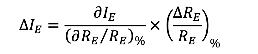
Thus, substituting the appropriate numerical values, we find that a 10% change in RE results in a 91.4 uA change in the emitter current of Q1. This is about 9.5% of its quiescent value of 967.0 uA.
Similarly, we can estimate the effect a 20% variation in transistor
BF has on the emitter current of Q1. Consider from the
above Spice generated sensitivities we see that ![]() A/%. Thus, a 20%
change in BF gives rise to a 5.39 uA change in the emitter current
of Q1. This is about 0.56% of the quiescent value.
A/%. Thus, a 20%
change in BF gives rise to a 5.39 uA change in the emitter current
of Q1. This is about 0.56% of the quiescent value.
It should be obvious that this same approach can be used for any of the components of the circuit in Fig. 4.23 whose sensitivities are given in the above table. One can also investigate the effect that different component changes has on the emitter current by making use of the mathematical concept of a total derivative. An example of this is provide in section 5.6 as it applies to a MOSFET amplifier circuit.
Sensitivity to Temperature Variations
To investigate the bias stability of an amplifier subject to temperature changes requires a different approach than that just seen using the sensitivity analysis (.SENS) command of Spice. For such cases, we make use of an extension to the DC sweep command which will allow the user to sweep the temperature of the circuit over a specified range while repeatedly performing a DC analysis. The syntax of this command is identical to any other DC sweep command with the keyword TEMP replacing the field marked by source_name. The range of temperature values is specified in exactly the same way as for a voltage or current source. For this particular example, we will monitor the emitter current over a temperature range beginning at 0°C and ending at 125°C in steps of 25°C. The exact syntax of this DC sweep command can be seen in the Spice input file for this example in Fig. 4.25.
|
Fig. 4.23: (a) An amplifier biased using a single power supply resistive network arrangement. (b) Monitoring the emitter current of the amplifier circuit by including a zero-valued voltage source (Vemitter) in series with the emitter of the transistor. (duplicate)
|
Investigating Emitter Current Dependence On Temperature
** Circuit Description ** * power supply Vcc 1 0 DC +12V * amplifier circuit Q1 2 3 4 Q2N2222A * resistive biasing network accounting for temperature dependence Rc 1 2 4k TC=1200u R1 1 3 80k TC=1200u R2 3 0 40k TC=1200u Re 4 5 3.3k TC=1200u Vemitter 5 0 0 * transistor model statement for the 2N2222A .model Q2N2222A NPN (Is=14.34f Xti=3 Eg=1.11 Vaf=74.03 Bf=255.9 Ne=1.307 + Ise=14.34f Ikf=.2847 Xtb=1.5 Br=6.092 Nc=2 Isc=0 Ikr=0 Rc=1 + Cjc=7.306p Mjc=.3416 Vjc=.75 Fc=.5 Cje=22.01p Mje=.377 Vje=.75 + Tr=46.91n Tf=411.1p Itf=.6 Vtf=1.7 Xtf=3 Rb=10) ** Analysis Requests ** * vary temperature of circuit beginning at 0C to 125C in temperature steps of 25C .DC TEMP 0 125 25 ** Output Requests ** .PLOT DC I(Vemitter) .probe .end
Fig. 4.25: The Spice input file for investigating the dependence of the emitter current on temperature in the amplifier circuit shown in Fig. 4.23.
|
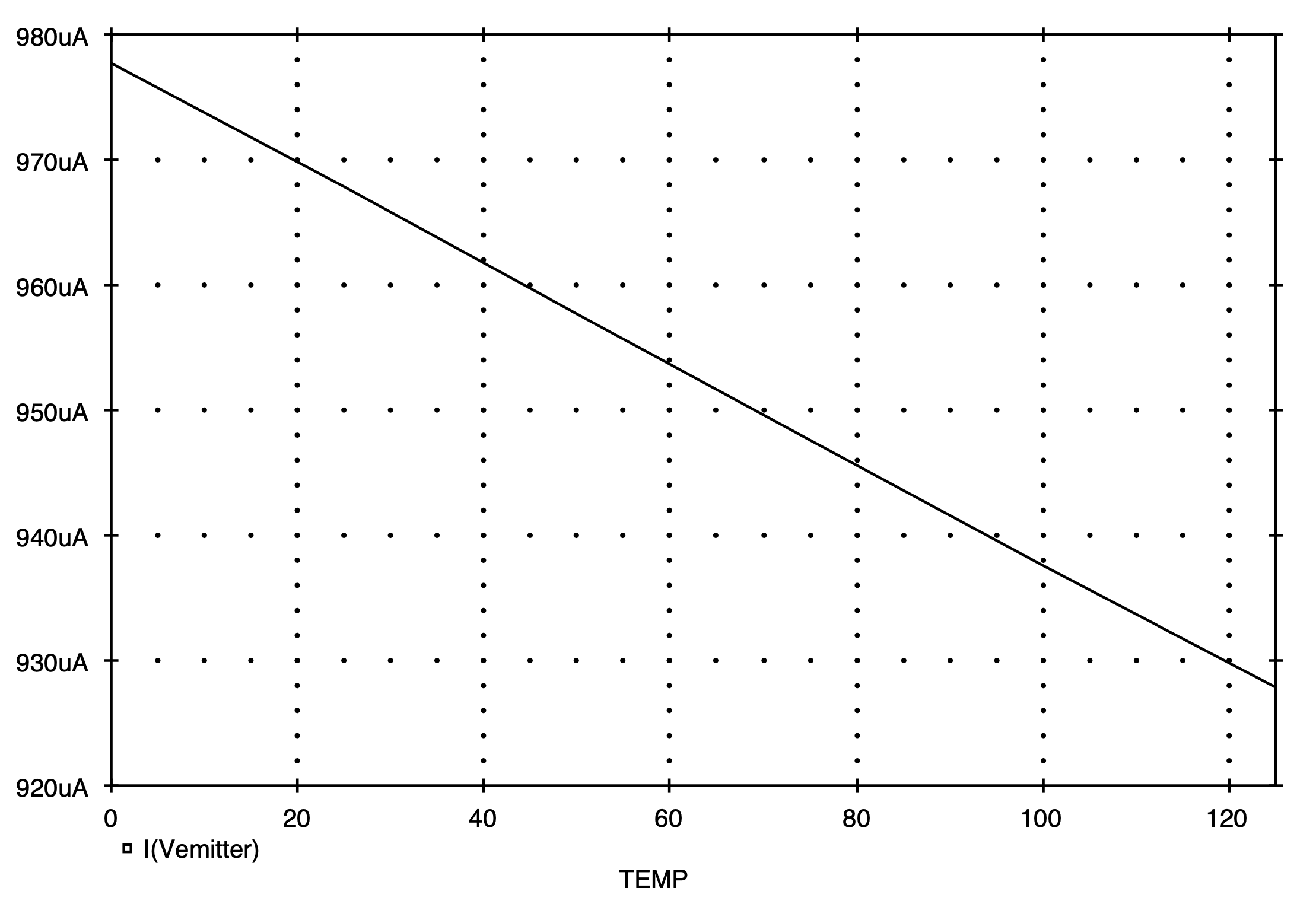
Fig. 4.26: Temperature variation of the emitter current in the amplifier circuit shown in Fig. 4.23(a).
The built-in model for the BJT accounts for variations in temperature. The same cannot be said for the resistors. In order to account for changes in resistance due to temperature variations, one must indicate on each resistor statement in the Spice input file its temperature dependence using the two temperature coefficients TC1 and TC2. The formula used by Spice to calculate the value of a resistor at a temperature (Temp) other than 27°C, is given by
(4.11)
![]()
For our purposes here, we shall consider only the linear dependence of resistance on temperature, and therefore, consider TC2=0. We shall assume for this example, that TC1 = 1200 ppm/°C, where ppm denotes parts-per-million or a multiplication factor of 10-6. To specify the dependence of a resistor on temperature in the Spice input file, one simply appends to the resistor statement, after the field indicating the nominal value of the resistor, TC=TC1. In this particular case, we will write TC=1200u. This is also indicated in the Spice input file listed in Fig. 4.25.
The results of the emitter current dependence on temperature are summarized in Fig. 4.26. For a 125°C change in circuit temperature, the emitter current changed by no more than 50 uA. This is sometimes expressed as a temperature coefficient in units of ppm/°C as the ratio of the change in emitter current divided by the emitter current at the nominal temperature of 27°C to the change in circuit temperature creating this current change. In this case, the emitter bias current has a temperature coefficient of -413 ppm/°C.
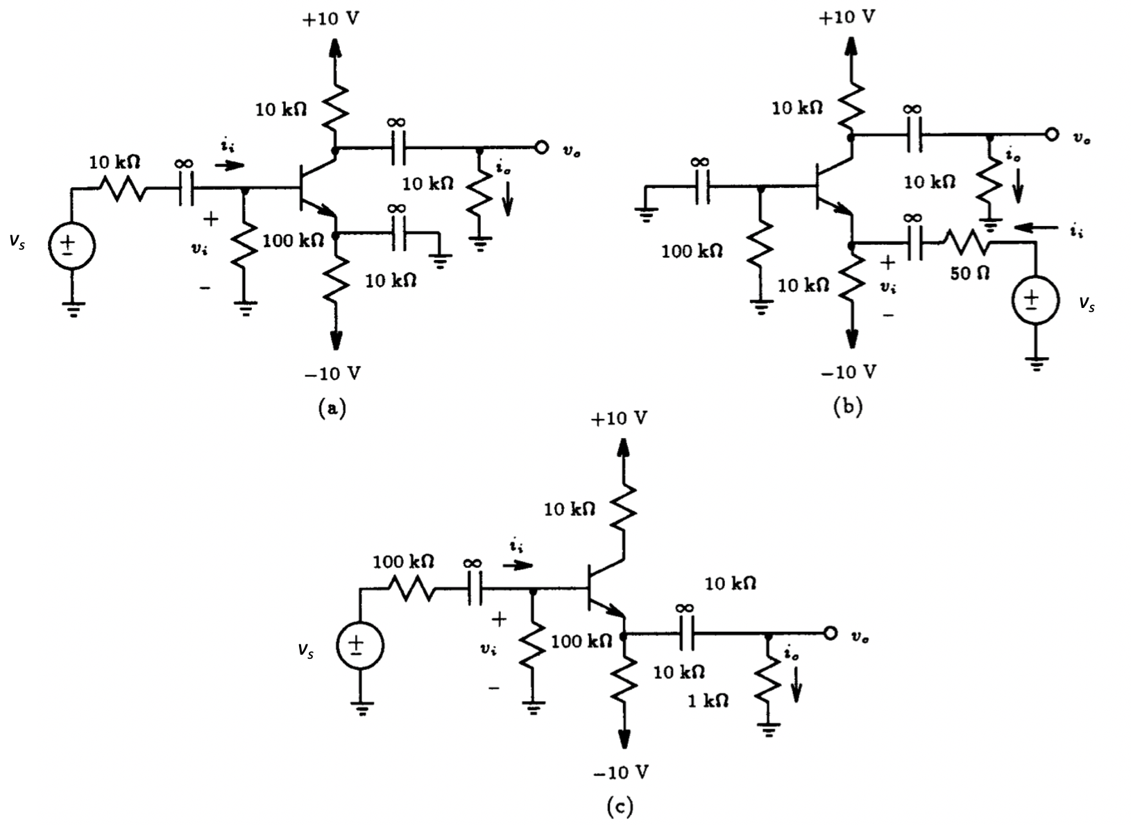
Fig. 4.27: Basic single-stage BJT amplifier configurations: (a) common-emitter amplifier, (b) common-base amplifier and (c) common-collector amplifier.
4.6 Basic Single-Stage BJT Amplifier Configurations
In this section we shall investigate the three basic types of amplifier configurations shown in Fig. 4.27: the common-emitter (CE), common-base (CB) and common-collector (CC). The primary goal of this section is to determine the small-signal parameters of these amplifiers, such as input resistance Ri, output resistance Ro, voltage gain Av and current gain Ai, using the AC analysis facility of Spice. These results will then be compared to those predicted by the formulae derived by hand in Sedra and Smith using small-signal analysis. The transistor used in each amplifier of Fig. 4.27 will be assumed modeled after the commercial 2N2222A npn transistor.
|
(a)
|
(b)
|


Fig. 4.28: Circuit setups used to determine the amplifier's small-signal parameters: (a) circuit arrangement for computing ii, vo and io (b) circuit arrangement for computing io due to voltage source connected to output terminal of amplifier.
The Common-Emitter Amplifier
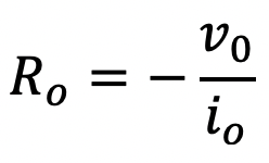
As the first example of this section, let us compute the small-signal parameters of the common-emitter (CE) amplifier shown in Fig. 4.27(a). To obtain all four parameters, i.e., Av, Ai, Ri and Ro, we will have to run two separate Spice analyses; one for computing the input current and the output voltage for a known voltage applied to the input of the amplifier, and the other for computing the current supplied by a voltage source connected to the output terminal of the amplifier when the input voltage source is set to zero. These two situations are depicted in Fig. 4.28. In order to monitor the current flowing through the load resistor we placed a zero-valued voltage source in series with it, as shown in Fig. 4.28(a). The input current to the amplifier can be determine by monitoring the current supplied by the input voltage source vs. The four parameters of the amplifier can then be computed from these results according to the following:
(4.12)
(4.13)
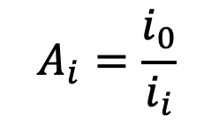
(4.14)
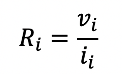
(4.15)
For the first case depicted in Fig. 4.28(a), consider applying a 10 mV AC signal to the input of the amplifier. A DC input voltage signal would not be useful here since the input source to the amplifier is AC-coupled. Thus, the frequency of the input signal should be selected to be in the midband frequency range of the amplifier. With the choice of decoupling and by-pass capacitors selected here (each selected very large at 1 GF)[1], an input frequency of 1 kHz is sufficiently midband. The Spice input file describing this circuit setup is provided in Fig. 4.29. Both a DC and an AC analysis requests are specified. The results of the AC analysis will be used to indirectly calculate the small-signal parameters of the amplifier, as mentioned above. The results of the DC analysis will provide us with the small-signal parameters of the transistor from which we can use the formulae derived in Sedra and Smith to predict the small-signal parameters of the amplifier and compare them to those computed by the indirect AC analysis approach.
|
(a)
Fig. 4.28: Circuit setups used to determine the amplifier's small-signal parameters: (a) circuit arrangement for computing ii, vo and io. (duplicate)
|
Common-Emitter Amplifier Stage
** Circuit Description ** * power supplies Vcc 1 0 DC +10V Vee 8 0 DC -10V * input signal Vs 6 0 AC 10mV Rs 5 6 10k * amplifier C1 4 5 1GF Rb 4 0 100k Q1 2 4 3 Q2N2222A Rc 1 2 10k Re 3 8 10k C2 2 7 1GF C3 3 0 1GF * load + ammeter Rl 7 9 10k Vout 9 0 0 * transistor model statement for the 2N2222A .model Q2N2222A NPN (Is=14.34f Xti=3 Eg=1.11 Vaf=74.03 Bf=255.9 Ne=1.307 + Ise=14.34f Ikf=.2847 Xtb=1.5 Br=6.092 Nc=2 Isc=0 Ikr=0 Rc=1 + Cjc=7.306p Mjc=.3416 Vjc=.75 Fc=.5 Cje=22.01p Mje=.377 Vje=.75 + Tr=46.91n Tf=411.1p Itf=.6 Vtf=1.7 Xtf=3 Rb=10) ** Analysis Requests ** * calculate DC bias point information .OP .AC LIN 1 1kHz 1kHz ** Output Requests ** * voltage gain Av=Vo/Vs .PRINT AC Vm(6) Vp(6) Vm(7) Vp(7) * current gain Ai=Io/Ii .PRINT AC Im(Vs) Ip(Vs) Im(Vout) Ip(Vout) * input resistance Ri=Vi/Ii .PRINT AC Vm(4) Vp(4) Im(Vs) Ip(Vs) .end
Fig. 4.29: The Spice input file for calculating the input current and the output voltage of the common-emitter amplifier shown in Fig. 4.28(a) subject to a 10 mV AC input signal.
|

Submitting the Spice input file for processing, we find on completion that the magnitude and phase of the input and output voltage of the amplifier is as follows:
|
**** AC ANALYSIS TEMPERATURE = 27.000 DEG C
FREQ VM(6) VP(6) VM(7) VP(7)
1.000E+03 1.000E-02 0.000E+00 5.068E-01 1.799E+02
|
Thus, we find that this amplifier has a midband voltage gain Av of -50.68 V/V. Likewise, the input and output currents associated with this amplifier are found to be:
|
**** AC ANALYSIS TEMPERATURE = 27.000 DEG C
FREQ IM(Vs) IP(Vs) IM(Vout) IP(Vout)
1.000E+03 6.803E-07 -1.796E+02 5.068E-05 1.799E+02
|
These two current results indicate that the midband current gain Ai of this amplifier is -74.49 A/A. Finally, the input resistance of the CE amplifier can be computed from the following results,
|
**** AC ANALYSIS TEMPERATURE = 27.000 DEG C
FREQ VM(4) VP(4) IM(Vs) IP(Vs)
1.000E+03 3.198E-03 -9.300E-01 6.803E-07 -1.796E+02
|
Thus, the midband input resistance Ri of this amplifier is 4.7 k-ohm.
Repeating this same process but with the input voltage source level set to 0 V and the level of the voltage source in series with the load resistance increased to 10 mV AC, we can determine the output resistance of this amplifier. This requires that we modify the statements for these two AC sources in the Spice deck seen listed in Fig. 4.29 to read as follows:
Vs 6 0 AC 0V
Vout 9 0 AC 10mV
Further, to access the resulting current supplied by the output voltage source Vout and the voltage developed across the output terminal of the CE amplifier, we include the following PRINT statement in the Spice deck:
.PRINT AC Vm(7) Vp(7) Im(Vout) Ip(Vout)
Re-running the Spice job, we find the following results in the output file:
|
**** AC ANALYSIS TEMPERATURE = 27.000 DEG C
FREQ VM(7) VP(7) IM(Vout) IP(Vout)
1.000E+03 4.728E-03 0.000E+00 5.272E-07 1.800E+02
|
From these results we compute the output resistance Ro to be 8.97 k-ohm.
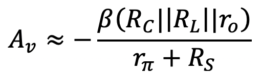
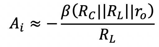
To compare the above results with those predicted by hand analysis, we list below the expressions for Av, Ai, Ri and Ro in terms of the small-signal model parameters of the transistor, as derived in section 4.11 of Sedra and Smith:
(4.16)
![]()
(4.17)
![]()
(4.18)
(4.19)
Here B is the small-signal transistor current gain[2] defined in terms of gm and rp according to:
(4.20)
![]()
With the inclusion of the .DC operating point command in the above mentioned Spice decks we find that the parameters of the hybrid-pi model for the 2N2222A transistor of the common-emitter amplifier are as follows:
|
**** BIPOLAR JUNCTION TRANSISTORS
NAME Q1 MODEL Q2N2222A IB 5.84E-06 IC 8.72E-04 VBE 6.42E-01 VBC -1.87E+00 VCE 2.51E+00 BETADC 1.49E+02 GM 3.36E-02 RPI 4.92E+03 RX 1.00E+01 RO 8.71E+04
|
Substituting the appropriate parameter value, together with values for the different circuit components, we find: Av=-52.3 V/V, Ai=-78.0 A/A, Ri=4.69 k-ohm and Ro=8.97 k-ohm. To compare these with those computed indirectly by Spice above, we list in Table 4.4 a comparison of the results of these two approaches. The first and second column of this table list the small-signal parameters of the amplifier and its formula in terms of the small-signal transistor model parameters. The third and fourth columns indicate the value predicted by hand analysis and that obtained indirectly with Spice. The fifth column indicates the relative difference between the two results as a means of indicating how accurate the hand analysis is. As is evident from the results listed in this table, the results compare quite well.
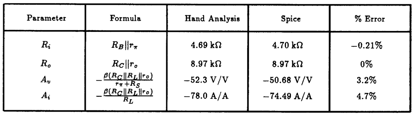
Table 4.4: Comparing the small-signal amplifier parameters of the common-emitter amplifier shown in Fig. 4.27(a) as calculated by hand analysis and that indirectly computed using Spice.
To demonstrate the usefulness of small-signal analysis, let us apply a small-amplitude sinusoidal signal to the input of the amplifier and observe the time-varying signal that appears at the output of this amplifier. Say for the sake of illustration, we apply a 10-mV sinusoidal of 1 kHz frequency to the input of the amplifier. The Spice deck for this particular situation is provided in Fig. 4.30. A transient analysis command is specified to compute the output waveform over three cycles of the input signal beginning at a time of 5 ms. This is to ensure that the circuit has had sufficient time to reach steady state. The dc-coupling and bypass capacitors have been assigned more practical values of 10 uF each, unlike those used in the previous AC analysis. In this way, the time to reach steady state is drastically reduced. One should note that by the very nature of a Spice transient analysis, the analysis performed here is a large-signal analysis and not a small-signal analysis even though the input signal level is small.
The results of the transient analysis are shown in Fig. 4.31. The top graph displays the 10-mV peak, 1 kHz input sinusoidal signal and the bottom graph displays the corresponding output signal. With the aid of Probe, we found that the amplitude of the output signal is 500 mV. Thus, the voltage gain of this amplifier is seen to be about -50 V/V, which agrees with that predicted by the two analyses above.
|
(a)
Fig. 4.28: Circuit setups used to determine the amplifier's small-signal parameters: (a) circuit arrangement for computing ii, vo and io.
(duplicate)
|
Common-Emitter Amplifier Stage With Sine-Wave Input
** Circuit Description ** * power supplies Vcc 1 0 DC +10V Vee 8 0 DC -10V * input signal Vs 6 0 SIN ( 0V 10mV 1kHz ) Rs 5 6 10k * amplifier C1 4 5 10uF Rb 4 0 100k Q1 2 4 3 Q2N2222A Rc 1 2 10k Re 3 8 10k C2 2 7 10uF C3 3 0 10uF * load + ammeter Rl 7 9 10k Vout 9 0 0 * transistor model statement for the 2N2222A .model Q2N2222A NPN (Is=14.34f Xti=3 Eg=1.11 Vaf=74.03 Bf=255.9 Ne=1.307 + Ise=14.34f Ikf=.2847 Xtb=1.5 Br=6.092 Nc=2 Isc=0 Ikr=0 Rc=1 + Cjc=7.306p Mjc=.3416 Vjc=.75 Fc=.5 Cje=22.01p Mje=.377 Vje=.75 + Tr=46.91n Tf=411.1p Itf=.6 Vtf=1.7 Xtf=3 Rb=10) ** Analysis Requests ** .OP .TRAN 50us 8ms 5ms 50us ** Output Requests ** .Plot TRAN V(7) V(6) .probe .end
Fig. 4.30: The Spice input file for calculating the time-varying output signal of the common-emitter amplifier subject to a 10 mV, 1 kHz sinusoidal input signal. Unlike the previous AC analysis, which is a small-signal analysis, a transient analysis performs a large signal analysis even when the input level is small.
|
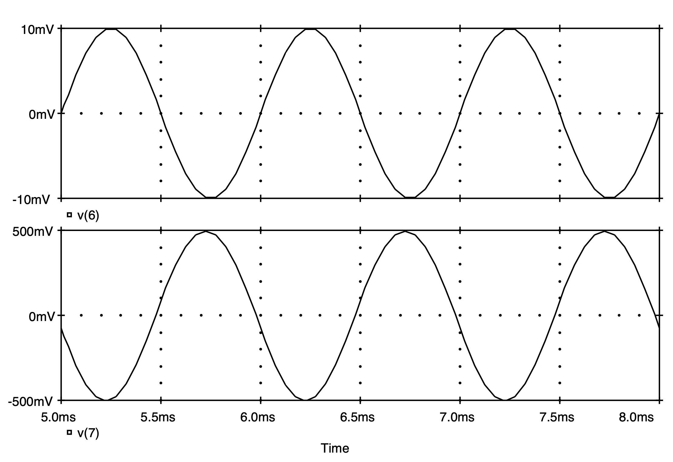
Fig. 4.31: The input and output time-varying voltage waveforms associated with the common-emitter amplifier shown in Fig. 4.27(a).
The Common-Base Amplifier
Another important amplifier configuration is the common-base (CB) amplifier shown in Fig. 4.27(b). Here the base of the transistor is AC grounded, the input signal source is connected to the emitter, and the load is connected to the collector. In the following we shall repeat the analysis method carried out on the common-emitter amplifier using Spice and compare the results with those estimated by the small-signal formulas derived by hand analysis.
The Spice input file for this common-base amplifier is shown in Fig. 4.32. Like the previous case of the common-emitter amplifier, a zero-valued voltage source is placed in series with the 10 k-ohm load resistor. This voltage source is used to monitor the current supplied to the load resistor. It will also be used to determine the output resistance of the amplifier. Both a DC and an AC analysis are specified. The DC analysis will provide us with the small-signal model parameters of the transistor. The AC analysis will enable us to determine the current supplied to the amplifier by the input voltage source, and the voltage and current supplied to the load resistor.
|
(b)
Fig. 4.27: Basic single-stage BJT amplifier configurations: (b) common-base amplifier.
(duplicate)
|
Common-Base Amplifier Stage
** Circuit Description ** * power supplies Vcc 1 0 DC +10V Vee 8 0 DC -10V * input signal Vs 6 0 AC 10mV Rs 5 6 50 * amplifier C1 4 0 1GF Rb 4 0 100k Q1 2 4 3 Q2N2222A Rc 1 2 10k Re 3 8 10k C2 2 7 1GF C3 3 5 1GF * load + ammeter Rl 7 9 10k Vout 9 0 0 * transistor model statement for the 2N2222A .model Q2N2222A NPN (Is=14.34f Xti=3 Eg=1.11 Vaf=74.03 Bf=255.9 Ne=1.307 + Ise=14.34f Ikf=.2847 Xtb=1.5 Br=6.092 Nc=2 Isc=0 Ikr=0 Rc=1 + Cjc=7.306p Mjc=.3416 Vjc=.75 Fc=.5 Cje=22.01p Mje=.377 Vje=.75 + Tr=46.91n Tf=411.1p Itf=.6 Vtf=1.7 Xtf=3 Rb=10) ** Analysis Requests ** * calculate DC bias point information .OP .AC LIN 1 1kHz 1kHz ** Output Requests ** * voltage gain Av=Vo/Vs .PRINT AC Vm(6) Vp(6) Vm(7) Vp(7) * current gain Ai=Io/Ii .PRINT AC Im(Vs) Ip(Vs) Im(Vout) Ip(Vout) * input resistance Ri=Vi/Ii .PRINT AC Vm(5) Vp(5) Im(Vs) Ip(Vs) .end
Fig. 4.32: The Spice input file for calculating the input current and the output voltage of the common-base amplifier shown in Fig. 4.27(b) subject to a 10 mV AC input signal.
|

Submitting the Spice input file for processing, we find on completion that the magnitude and phase of the input and output voltage of the amplifier are as follows:
|
**** AC ANALYSIS TEMPERATURE = 27.000 DEG C
FREQ VM(6) VP(6) VM(7) VP(7)
1.000E+03 1.000E-02 0.000E+00 6.096E-01 -6.826E-05
|
Therefore, we determine that this common-base amplifier has a midband voltage gain Av of +60.96 V/V. Likewise, the input and output current associated with this amplifier are found to be:
|
**** AC ANALYSIS TEMPERATURE = 27.000 DEG C
FREQ IM(Vs) IP(Vs) IM(Vout) IP(Vout)
1.000E+03 1.231E-04 1.800E+02 6.096E-05 -6.826E-05
|
Thus, the input current to the amplifier is 123.1 uA and the current supplied to the load is 60.96 uA, giving a current gain 0.495 A/A. Finally, the input resistance of the CB amplifier can be computed from the following results,
|
**** AC ANALYSIS TEMPERATURE = 27.000 DEG C
FREQ VM(5) VP(5) IM(Vs) IP(Vs)
1.000E+03 3.845E-03 1.819E-03 1.231E-04 1.800E+02
|
Thus, the midband input resistance Ri is 31.2 ohm.
Repeating this same process but with the input voltage source level set to 0 V and the level of the voltage source in series with the load resistance increased to 10 mV AC, we find that the output resistance Ro of this amplifier is 9.58 k-ohm. This was found from another Spice run of a modified version of the Spice deck shown in Fig. 4.32 where the two AC input and output voltage sources were modified to read as follows:
Vs 6 0 AC 0V
Vout 9 0 AC 10mV
and the following PRINT statement was added to the Spice deck:
.PRINT AC Vm(7) Vp(7) Im(Vout) Ip(Vout)
The results of this analysis are then found below:
|
**** AC ANALYSIS TEMPERATURE = 27.000 DEG C
FREQ VM(7) VP(7) IM(Vout) IP(Vout)
1.000E+03 4.894E-03 0.000E+00 5.106E-07 1.800E+02
|
As a means of comparison, we summarize in Table 4.5 the small-signal formulae pertinent to the common-base amplifier derived by hand in Sedra and Smith, together with their values as calculated by substituting the relevant transistor small-signal model parameters into each equation. The small-signal model parameters for the 2N2222A transistor are identical to those found in the common-emitter case in the previous subsection. This is not too surprising given that the transistor of the common-base amplifier is biased in exactly the same manner as in the common-emitter amplifier. This was also confirmed by the DC analysis performed by Spice on the common-base amplifier. A fourth column is also included in this table listing the small-signal parameters computed from the Spice analysis above. As is evident from the fifth column, indicating the relative error between the two methods of estimating the amplifier small-signal parameters, we see that they are in good agreement.
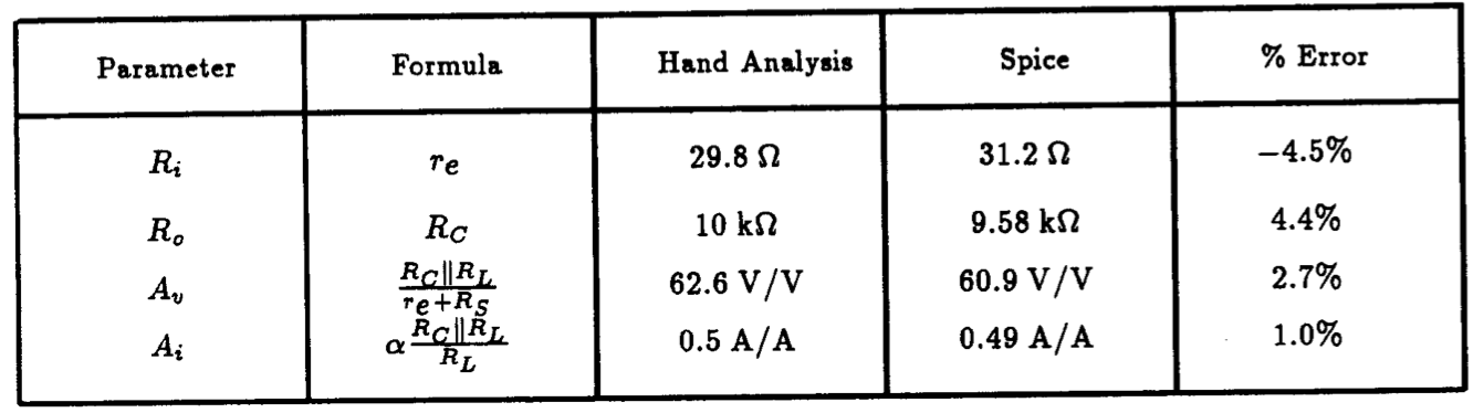
Table 4.5: Comparing the small-signal parameters of the common-base amplifier shown in Fig. 4.27(b) as calculated by hand analysis to those indirectly computed using Spice.
Table 4.6: Comparing the small-signal parameters of the common-collector amplifier shown in Fig. 4.27(c) as calculated by hand analysis to those indirectly computed using Spice.
The Common-Collector Amplifier
This same analysis can be repeated for the common-collector (CC) amplifier configuration shown in Fig. 4.27(c). Rather than list much of the same as that seen previously, we simply summarize the results in Table 4.6. As before, the Spice results are in good agreement with those obtained with hand analysis.
4.7 The Transistor as a Switch
As the final example of this chapter, consider the simple transistor switching circuit shown in Fig. 4.33. This particular circuit was designed by Sedra and Smith in Example 4.14 of their text such that transistor Q1 is in saturation with an overdrive factor larger than 10 when the transistor has a minimum B of 50. With the aid of Spice, we would like to determine the overdrive factor of the transistor in this circuit when the transistor is assumed to be the commercial 2N696 npn device and the base driving voltage VBB equals 5 V.
The overdrive factor (OD) of a saturated transistor is defined as the ratio of the base current IB divided by the minimum base current that will force the transistor into saturation, denoted as IBsat. Thus,
(4.21)
Correspondingly, at the minimum base current condition, the transistor is beginning to conduct a collector current ICsat. Moreover, as the device is driven further into saturation the collector current remains fairly constant at ICsat. Thus, the point at which the collector current begins to saturate denotes the edge of the saturation region. Using Spice, we shall compute the input condition that gives rise to the transistor entering its saturation region in the circuit of Fig. 4.33. This can be accomplished by sweeping the base driving voltage VBB between ground and 5 volts and observing both the collector current and the base current of the transistor. From this, we can then determine the base current IBsat. Moreover, at VBB=5 V, we can determine the base current IB and thus the overdrive factor OD for this particular circuit.
|
(b)
Fig. 4.33: A simple transistor switching circuit (Example 4.14 of Sedra and Smith).
|
Example 4.14: Using The 2N696 As A Switch
** Circuit Description ** * power supplies Vcc 1 0 DC +10V * input signal Vbb 4 0 DC +5V * transistorized switch Q1 2 3 0 Q2N696 Rc 1 2 1k Rb 4 3 2.2k * transistor model statement for the 2N696 .model Q2N696 NPN (Is=14.34f Xti=3 Eg=1.11 Vaf=74.03 Bf=65.62 Ne=1.208 + Ise=19.48f Ikf=.2385 Xtb=1.5 Br=9.715 Nc=2 Isc=0 Ikr=0 Rc=1 + Cjc=9.393p Mjc=.3416 Vjc=.75 Fc=.5 Cje=22.01p Mje=.377 Vje=.75 + Tr=58.98n Tf=408.8p Itf=.6 Vtf=1.7 Xtf=3 Rb=10) ** Analysis Requests ** .DC Vbb 0V 5V 0.1V ** Output Requests ** .PLOT DC I(Vcc) I(Vbb) .probe .end
Fig. 4.34: The Spice input file for calculating the overdrive factor associated with the switching circuit shown in Fig. 4.33. The transistor is modeled after the commercial npn transistor 2N696.
|

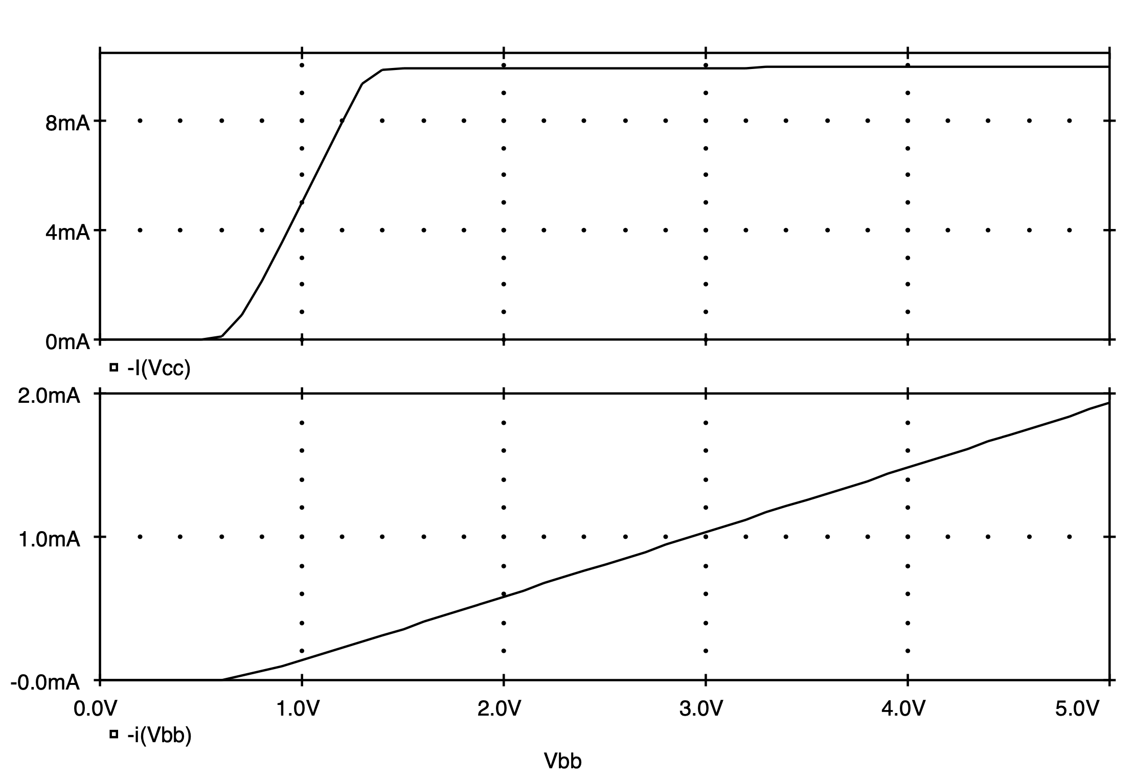
Fig. 4.35: The collector and base current characteristics of the transistor in the circuit of Fig. 4.34 as functions of the base driving voltage VBB. The top curve displays the collector current and the bottom trace displays the base current.
The Spice input file for the switching circuit shown in Fig. 4.33 is listed in Fig. 4.34. A DC sweep analysis is requested that varies the input voltage VBB between 0 and 5 volts in 0.1-volt increments. The BJT model parameters for the 2N696 npn transistor are also listed. These were derived from nominal device characteristics.
The results of the Spice analysis are shown plotted in Fig. 4.35. The upper trace displays the transistor collector current IC as a function of the base driving voltage VBB, and the lower trace displays the corresponding base current for the same input voltage. Using the cursor feature in Probe we find from the plot of collector current that the collector current begins to saturate at a current level of 9.79 mA when the base driving voltage VBB exceeds 1.4 V. Correspondingly, from the trace of the transistor base current, we find that at an input voltage VBB of 1.4 V, the base current is 313.6 uA. Hence, IBsat=313.6 uA. Also, we find at an input voltage level of VBB=5 V, the transistor base current IB is 1.932 mA. Therefore, using Eqn. (4.21), we compute the overdrive factor OD for transistor Q1 to be 6.16.
4.8 Spice Tips
· A BJT is described to Spice using an element statement and a model statement.
· The element statement describes how the base, collector, and emitter of a transistor are connected to the rest of the network.
· The model statement contains a list of parameters describing the terminal characteristics of a BJT using the built-in model of Spice.
· There are 40 parameters associated with the built-in Spice model of the BJT. (We discussed only 6 of them, the remainder are described in the Appendix).
· A specific transistor mode of operation is deduced from the DC voltages that appears across its emitter-base junction and collector-base junction. This information can be found in the Spice output file as a result of an operating point (.OP) analysis.
· When an operating point (.OP) calculation is included in the Spice input file, a list of operating point information for each transistor is obtained. This information contains DC bias conditions for the transistor and the parameters associated with its small-signal model.
· Models of many commercial bipolar transistors are available from various semiconductor manufacturers. A library of transistor models for various commercial transistors are available with the PSpice program.
· Spice can be used to generate families of {\it i-v} curves for transistors, just like the laboratory curve-tracer instrument.
· A DC sweep command can be extended to include a sweep of temperature, allowing one to investigate the circuits dependence on temperature.
· The pulse width of a time-varying waveform generated by the PULSE source statement of Spice cannot be made equal to zero. Instead, a value that is much smaller, at least several orders of magnitude less, than the period of the waveform is assigned to the pulse width.
· The DC sensitivities of a circuit can be computed using the .SENS analysis command. This command will compute the sensitivities of a particular circuit variable to most of the components in the circuit. This includes the sensitivities of many of the model parameters of the BJT.
· If the effect of decoupling and by-pass capacitors is to be ignored then their values should be selected to be very large during the simulation (generally, a good value is 1 GF).
4.9 Bibliography
L. W. Nagel, SPICE2 - A computer program to simulate semiconductor circuits, Memorandum no. ERL-M520, May 1975, Electronic Research Laboratory, University of California, Berkeley.
N. R. Malik, Determining Spice parameter values for BJT's, IEEE Transaction on Education, vol. 33, No. 4, pp. 366-368, Nov. 1990.
4.10 Problems
4.1. Consider the case of a transistor whose base is connected to ground, the collector is connected to a 10 V dc source through a 1 k-ohm resistor, and a 5-mA current source is connected to the emitter with the polarity so that current is drawn out of the emitter terminal. If BF=100 and IS =10-14 A, find the voltages at the emitter and the collector using Spice. Further, determine the base current.
4.2. Using the Spice model parameters for the commercial 2N2222A npn BJT given in Section 4.5, determine its leakage current ICBO at room temperature (i.e., 27°C). If the temperature of the device is raised to 75°C, what is the new ICBO? {\it Hint: Connect the base to ground, the collector to +5 V, and do not connect the emitter terminal. The current supplied by the +5 V voltage source is ICBO.
4.3. Consider a pnp transistor having IS=10-13 A and BF=40. If the emitter is connected to ground, the base is connected to a current source that pulls out of the base terminal a current of 10 uA, and the collector is connected to a negative supply of -10 V via a 10 k-ohm resistor, find the base voltage, the collector voltage, and the emitter current using the operating point (.OP) command of Spice.
4.4. Using Spice as a curve tracer, plot the iC - vCE characteristics of an npn transistor having IS=10-15 A and VA=100 V. Provide curves for vBE=0.65, 0.70, 0.72, 0.73 and 0.74 volts. Show the characteristics for vCE up to 15 V.}
4.5. For a BJT having an Early voltage of 200 V, what is its output resistance at 1 mA as calculated by Spice? at 100 uA?
4.6. The transistor in the circuit of Fig. P4.6 has a very high BF (assume at least 106 in the Spice file). The other parameters of the transistor Spice model can assume default values. Find VE and VC for VB equal to (a) +3 V, (b) +1 V, and (c) 0 V. What is the transistor mode of operation in each case?
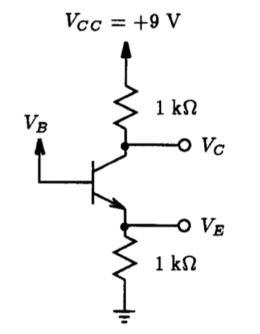
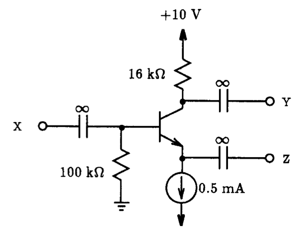
Fig. P4.6 Fig. P4.9
4.7. For the circuit in Fig. P4.6, with the aid of Spice and VB set equal to +2 V, find all node voltages for (a) BF very high (>106), and (b) BF=99.
4.8. In the circuit of Fig. 4.16, the input signal vi is described by 0.004 sin(wt) volts and the transistor is assumed modeled after the 2N2222A type. In addition, VBB is reduced from 3 V to 1 V. Using Spice, plot the base and collector current of Q1 as a function of time for at least one period of the input signal. Likewise, plot the collector voltage of Q1. What is the voltage gain of this amplifier?
4.9. The transistor shown in the circuit of Fig. P4.9 has BF=100 and VA=80 V. Use Spice to answer the following questions, but also compare your results with those obtained through a hand analysis:
a) Find the dc voltages at the base, emitter, and collector using Spice. Represent the infinite-valued capacitors with a very large, but finite, value.
b) Find gm, rp, and ro.
c) If terminal Z is connected to ground, X to signal source Vs having a 10 k-ohm source resistance, what is the voltage gain vy/vs. Since the capacitor connected to node Y is left floating, either connected a large load to node Y or remove this capacitor and take the measurement directly from the collector of the transistor.
d) If terminal X is connected to ground, Z to an input signal source vs having a 200 ohm source resistance, and Y to a load resistance of 10 k-ohm, find the voltage gain vy / vs.
e) If terminal Y is connected to ground, X to an input signal source vs having a 100 k-ohm source resistance, and Z to a load resistance of 1 k-ohm, find the voltage gain vz / vs.
4.10. With the aid of Spice, verify the design of a version of the circuit in Fig. 4.23 that uses ±9.5 V supplies for operation at 10 mA (for high BF), such that the total variation in IE is less than 5% for BF as low as 50. To obtain the highest possible voltage gain, select the largest possible value for RC; however, you must ensure that VCE is never less than 2 V.
Fig. P4.11
4.11. For the common-emitter amplifier shown in Fig. P4.11, let VCC=9 V, R1=27 k-ohm, R2=15 k-ohm, RE=1.2 k-ohm, and RC=2.2 k-ohm. The transistor has BF=100 and VA=100 V. Using Spice, calculate the dc bias current IE. If the amplifier operates between a source for which Rs=10 k-ohm and a load of 2 k-ohm, determine the values of Ri, Gm, Ro, Av, and Ai.
4.12. Repeat Problem 4.11 with the transistor modeled after the commercial transistor 2N696. Use the Spice parameters for the 2N696 provided in Section 4.6.
Fig. P4.13
4.13. The amplifier of Fig. P4.13 consists of two identical common-emitter amplifiers connected in cascade.
a) For VCC=15 V, R1=100 k-ohm, R2=47 k-ohm, RE=3.9 k-ohm, RC=6.8 k-ohm, and BF=100, determine the dc collector current and collector voltage of each transistor using Spice. The amount of data that must be typed into the computer is reduced if a subcircuit is created for one of the stages and used twice to form the overall amplifier.
b) Find Rin1 and vb1/vs for Rs=5 k-ohm.
c) Find Rin2 and vb2/vb1 for Rs=5 k-ohm.
d) For RL=2 k-ohm, find vo/vs.
Fig. P4.14
4.14. For the emitter-follower circuit shown in Fig. P4.14 the BJT used is specified to have BF values in the range of 20 to 200. For the two extreme values of B find:
a) IE, VE and VB.
b) the input resistance Ri.
c) the voltage gain vo/vs.
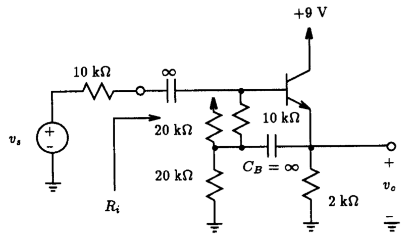
Fig. P4.15
4.15. For the bootstrapped follower circuit shown in Fig. P4.15 where the transistor is assumed to be of the 2N2222A type, compare the input and output resistance, and the voltage gain vo/vs, with and without the bootstrapping capacitor CB in place.
4.16. One small-signal BJT model parameter that is used in the small-signal calculations of Spice but is not sent to the Spice output file when an .OP command is specified is ru. Devise a simple circuit arrangement for calculating this small-signal resistance with Spice.